M4 Board – Retrofun, 8-Bit Amstrad CPC WiFi

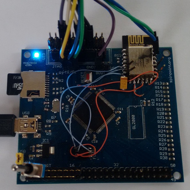
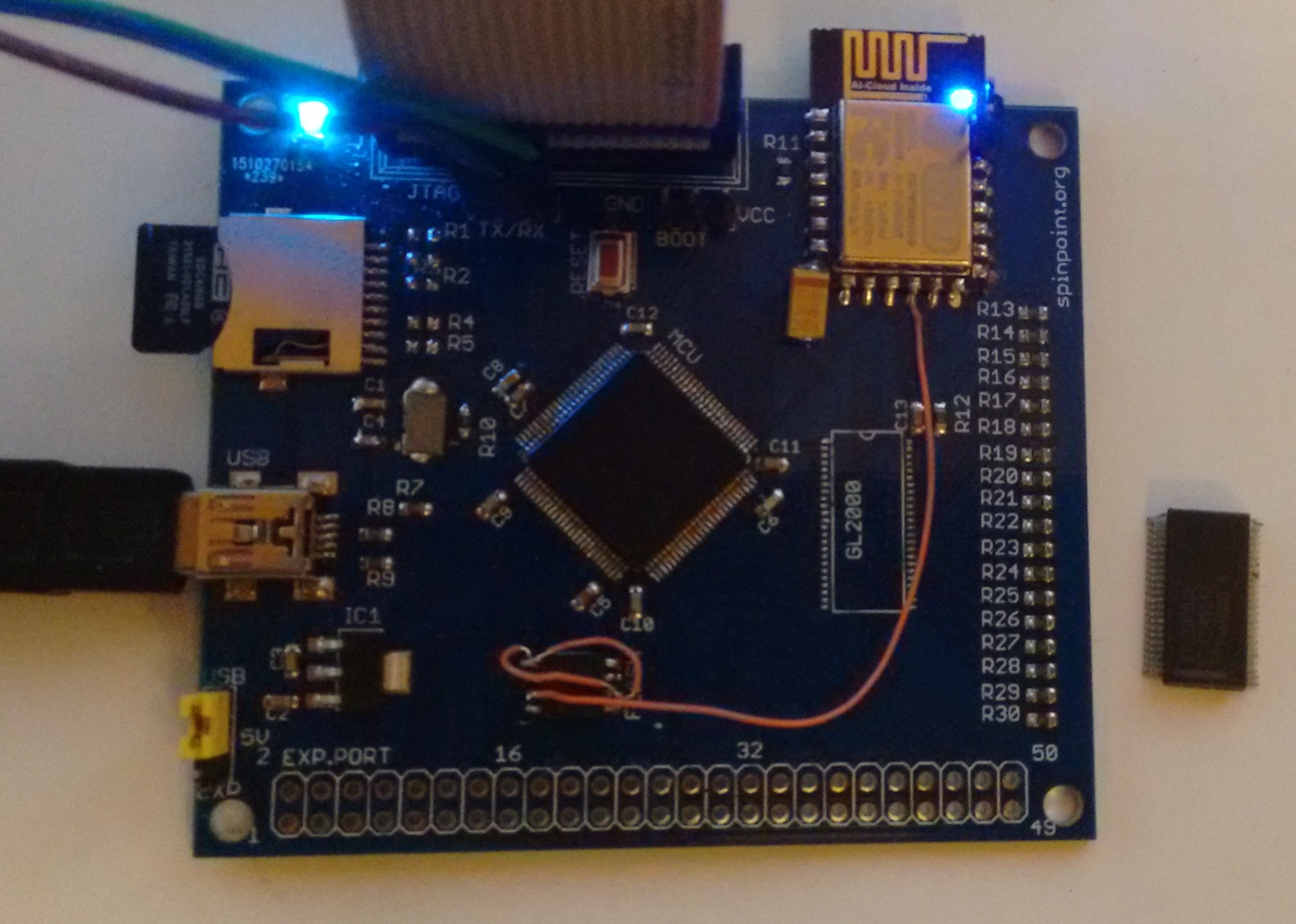
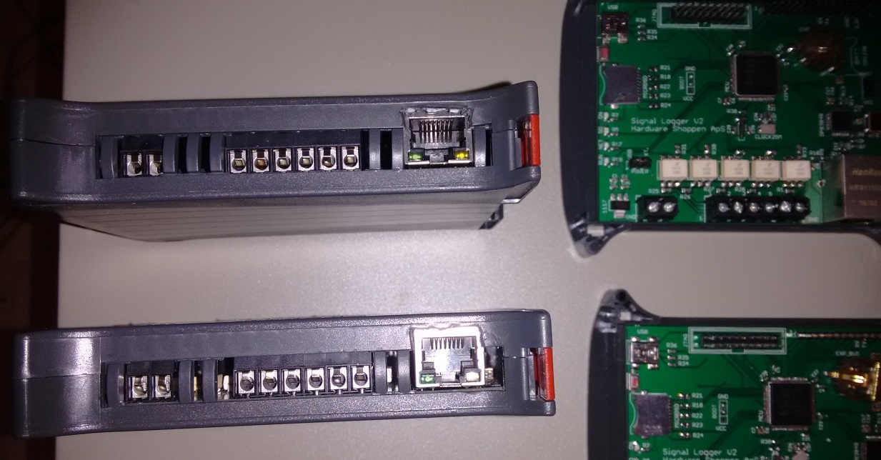
Description and purpose of the “M4 board”.
m4board_v2
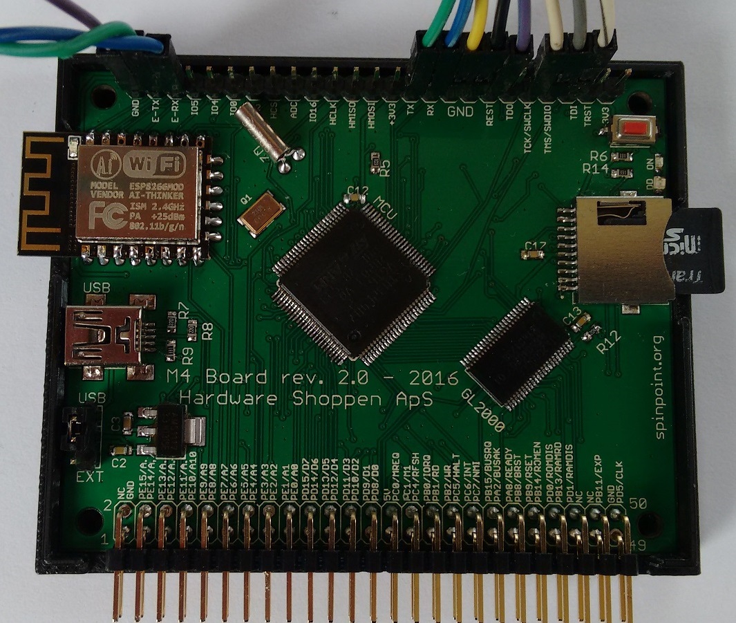
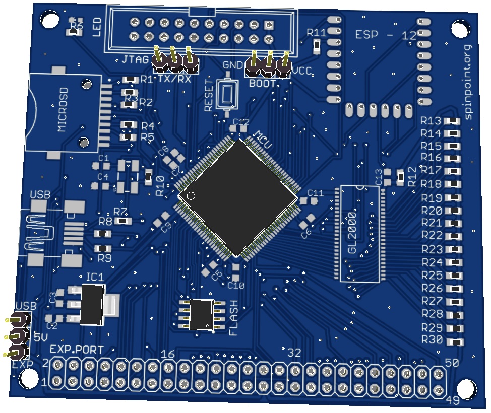
The M4 board, features as previously described a ST32F407 Cortex M4 MCU, connected via SPI to a ESP8266 WIFI module, and 18 GPIO’s routed via a GTL2000 voltage translator chip.

It was meant to be connected to the old the Amstrad CPC (z80 based) computer via it’s expansion port.
As with most old age computers, it runs with 5V I/O, here is where the GTL2000 chip came in handy.
The signals driven through the GTL2000 are output signals and the bi-directional data bus (D0-D7).

Input signals are connected directly to the ST32F407 Cortex M4 as it is 5V tolerant.

The idea was to provide WiFi to the Amstrad CPC, for easy and fast data exchange between it and a PC, but also direct internet access.

ROM BOARD emulation
First prerequisite was the ability to run code on the Amstrad via the M4 MCU so no additional loading (i.e. disc) would be needed.
It would be done by mapping a ROM in the Amstrad addressable space, this ROM would be in the M4 ram.

IORQ and WR will occur when a ROM is selected, data lines will contain the ROM number.
ROMEN and RD will occur when a read is happening from the currently selected ROM, address lines have the address, ROM data will be send back over the data lines.
A fairly trivial task, but the timing is tight having to bit bang the gpio, do direction changes on gpio’s mapped as data lines, even when the bus runs at only 4MHz.
Much time spent optimizing the handler in ARM assembler, it finally worked.

SD card storage
Being able to run code via the ROM board emulation, it would be nice to have native r/w storage.
A micro SD card slot connected to the M4 SDIO lines, was meant for this purpose.
An transfer interface from the Amstrad CPC to the M4 was designed.
Two I/O ports were assigned when an IORQ happened, one for receiving data on the M4 and one for telling it data was send, so it could process.
This was done as it’s easy to store data (low clock count), but takes additional time to process them.
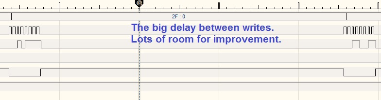
When the 2nd port is written, the MCU sends BUSRQ signal to the Z80 CPU, which will ‘freeze’ the z80 CPU at the end of the current cycle, now the M4 has the time it needs to process the incoming data, before resuming the Z80 CPU and responding.
Responses are done in the ROM space, which of course is read only on the CPC, but R/W on the M4, as it is kept in the M4 ram!
Next up, was to hook the system bios/firmware functions, that do file related I/O to tape and disc on the original system and re-directing them to the sdcard.
Thus native file access from the SD card is possible, providing the CPC with up to 32GB (or more) of storage via SD card.

WiFi & Internet
In short the connection between ESP8266 and the M4 was done via SPI as IPC.
To allow internet/WiFi access from the Amstrad CPC itself, it sends a command to the M4, which again sends an IPC call to the ESP.
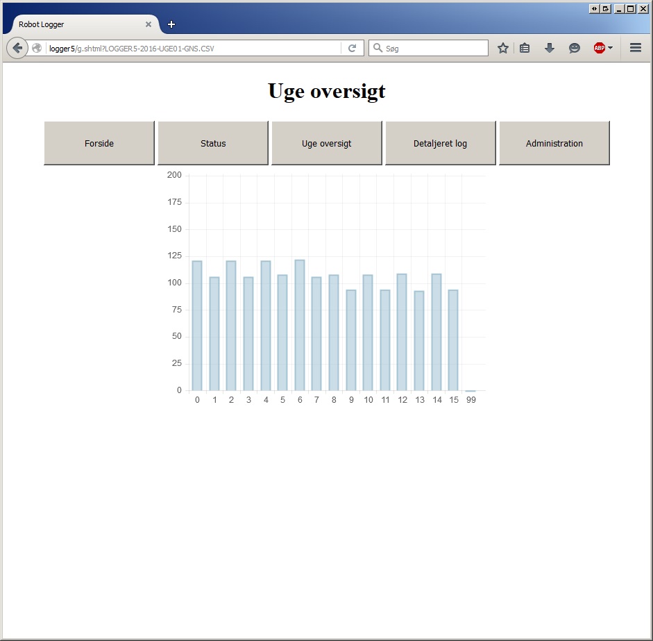
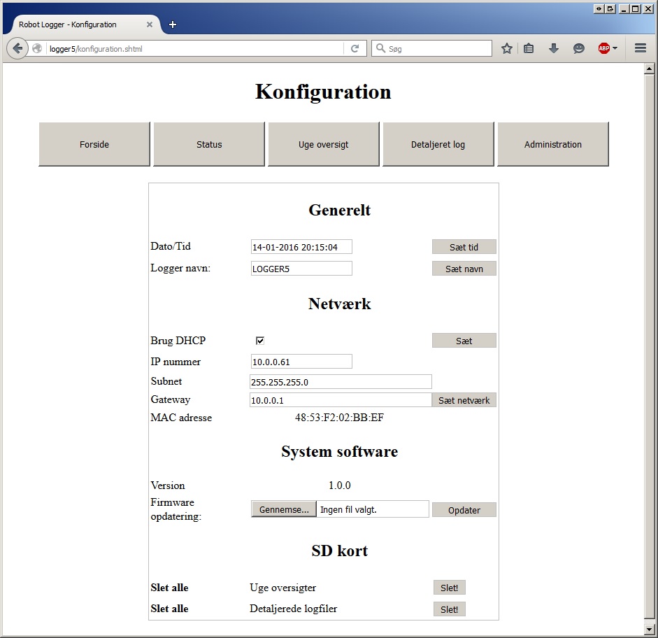
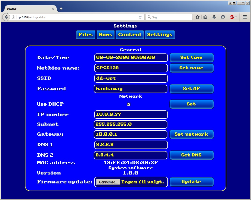
WEB interface
The ESP8266 hosts a WEB server, where various settings can be altered.
web_interface1 web_interface2

RTC
A battery mount was put on the board, making it possible to provide Real time clock as well via the RTC in the ST32F407.

What it does
Emulate Romboard, currently up to 16 roms, can be uploaded/removed via Web Interface.
Download files from internet via WiFi.
Mass storage to SD card, via native file I/O. R/W support. Emulated as drive A.
Can use DSK files on the SD card too, but only for file read access and sector reading via firmware call.
Upload files via web interface.

See a short demonstration here:

To do
Finish commands.
Lots of error checking.
Bug fixing.
More commands.
Other features.
hooked_up_to_la
Should anyone be mad enough to want a similar interface for their Amstrad CPC (or other suggestions), don’t hesitate to put a comment.
If enough are interested, I will run a batch + it’ll motivate me to finish and polish things up.

-Duke

M4 Board – The SPI IPC

A little progress on the M4 Board, I managed to get the IPC (inter processor comms) system between the Cortex-M4 and the ESP8266 going.
It uses HSPI interface + GPIO0 on the ESP and SPI1 interface + a gpio on the M4.

SPI comms from ESP to Cortex-M4
Cortex-M4 acts as spi-slave, it will listen to the any incoming HSPI command from the ESP, via SPI_RXNE interrupt (on SPI1 irq handler, max. 42 MHz).
The irq handler is done with some very optimized assembler code and simply buffers whatever is send from the ESP, whenever there is something in the rx buffer. It also deals with sending any data if there is something in the transmit buffer to send.
HSPI CS will trigger an external interrupt on both edges on the M4.
When HSPI CS goes low, it will clear the index of the spi1 rx buffer.
When HSPI CS goes high, it will process the command/data received in the spi1 buffer.

Cortex-M4 to ESP
GPIO0 is set as input on the ESP and the M4 will pull this low whenever it wants to send command/data to the ESP. Prior to that command and data is written to the transmit buffer of the SPI IRQ handler.
This triggers an interrupt on the ESP, which will then start clocking dummy data out on the SPI to read/process the responses (full duplex).
This wont come in any faster than the ESP is driving the clock. The HSPI clock is set to 40 MHz.

Results
This system works pretty well now. It’s not as fast as I’d like. Currently transfer is about 500 KB/s, while I can download to the ESP with about 900KB/s under optimal conditions.
So the SPI IPC is a bottleneck, however there is still room for improvement.
As the clock speed is really fine on the SPI, the problem is the delay between each byte write from the ESP which is done via CPU writes.
Ideally I could use DMA, but there seems to be no info on this anywhere in regards to the ESP.
Another option is to use 16 bit read/writes instead of 8 bits and probably almost double the speed.
Or I could use the entire 64 byte buffer of the ESP HSPI interface and clock them out nicely without delays 64 bytes at a time.

Other
On the hardware side, I have re-designed the board and ordered new pcb’s. I screwed up the footprint of the GTL2000 chip and there simply was no way about. Obviously other improvements & fixes were added.

– Duke

spi_delaym4board_mess

M4 Board – update #2

After ages of waiting for components to arrive from China (and some didn’t, so I had to reorder).
I was finally ready to assemble the M4 board. After applying the solder mask and doing pick and place, I found the GL2000 bi-directional level converter was the wrong package :/  – Oh well added the other components as there is enough work to do without it for now. Also a couple of other screwups, ie. swapped miso and mosi on the flash, used wrong SCK pin on ESP-12E (notice it is PIN 12 that’s spi-clock). So eventually I will have to re-do the PCB.
Update: It’s not entirely true, it is because there is two (known) different ESP-12E modules in existence, see here http://www.esp8266.com/viewtopic.php?f=5&t=3163   My initial layout wasn’t wrong, I just got a 12E module with a different pin layout :/

For now, the MCU, SD and SPI flash is working, I can access the ESP8266 wifi chip and read/write the spi flash from the Cortex M4 (keep the ESP in reset state and do spi access) and obviously send serial commands.
However the plan is to make an IPC interface via SPI between the Cortex M4 and the ESP-8266 to get proper performance.
I will update on this as I get along.

-Duke

m4board_upd2

PLC datalogger

A side project to log industrial robots via their PLC (24V) interface.

The PCB consists of:

  • ST32F407VGT (Cortex M4) as the MCU.
  • SD card for storing detailed logs.
  • DP83848 ethernet PHY hooked up to the M4 RMII interface, connecting it to the LAN, so logs can be downloaded, statistics viewed, live view, settings and more.
    Using netbios names and DHCP by default, so easily accessible without pre-setting.
  • Optocouplers to completely seperate the PLC signals from the board.
  • Battery backup for SRAM and RTC, even poweroff’s are logged.
  • Status leds for Power On, SD card OK, Ethernet OK, MCU running (flashing).
  • Firmware upgradable from LAN/Internet or microSD.

The PCB was designed to fit a compact DIN rail case and using screw terminals for power and PLC signals.
For once it was a really smooth experince, only screwed up the battery polarity, which was easily fixed by using another holder.

logger_pcb logger_case logger_screenshot2 logger_screenshot1

USB3FPGA assembled

After a long wait, the last components for the USB 3.0 to FPGA board arrived. Board is now reflown.
Both ends work, Spartan 6 FPGA detected via JTAG and FT601Q detected via USB3.0.
Being occupied with a few other projects at the moment, it probably will take a bit before I have time to write the appropriete VDHL and Windows D3XX code to fully test it. Hopefully in a few weeks I’ll be able to get some realtime fast data acquisition going with it.

-Duke
usb3fpga_reflown2 ft601q_conf fpga_found

T962A – Reflow oven upgrade!

Thanks to the hard work of the guys over at UnifiedEngineering there is now an improved opensource firmware available for the T962A reflow oven.
The hack was also featured on hackaday last year.
Finally upgraded mine, soldering in the DS18B20 temperature sensor and routing out the ICSP connector, so the firmware can be reflashed via a serial connection. I used the widely available FT232 and Flash Magic software.
Still need to replace the masking tape and perhaps add the fan control too.
Update: Replaced the masking tape with kapton heat resisting tape.
Cool stuff indeed -:)
T962A_1 T962A_2 T962A_3 T962A_4 T962A_5kapton_tape

Cortex M4 board

Having a few spare ST32F407 chips collecting dust, I decided to make a neat little board for it. Featuring USB, JTAG, microSD, 32Mbit spiflash, WiFi,  18 GPIOS with 3.3V / 5V bi-directional level translation for a special purpose 🙂
Cortex-M4 is a great ARM MCU running at 168MHz, 192KB ram and 1MB flashrom. The one in use is a ST32F407VGT in a TQFP100 package, all GPIO’s are routed, no components backside. Board size 76×66 mm.
cortexm4

Still waiting for my USB3.0 FPGA boards to arrive.

USB 3.0 FPGA board

Done the pcb, just need to fix up the silkscreen and re-check everything before sending it to a fab house. Now sent to pcb manufacturer.
The board features the FT601Q Super speed (QFN76, 9x9mm!) connected to an Xilinx Spartan 6SLX9TQG144 FPGA.
All routed in 2 layers – yeah I know it’s not pretty, I am just happy if it works…

-Duke
usb30fpga2

FTDI FT601Q

Just made an Eagle library for the USB3.0 fifo chip FT601Q, that I am planning to use for a board. More info about the SuperSpeed USB3.0 chip over at  FTDI chips.

Attached the Eagle lbr here in case anyone wants to save some time.
Notice it’s untested as of now.

ft601q

-Duke

ft601q_1 ft601q_2